
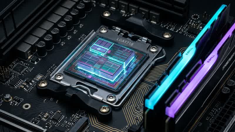
When evaluating gaming CPUs, average frame rate charts only tell half the story. In CPU-bound titles—such as Baldur's Gate 3 (Act 3 Lower City), Factorio, Stellaris, Microsoft Flight Simulator, Escape from Tarkov, and World of Warcraft raids—the difference between a smooth experience and micro-stutter lies in 1% and 0.1% low frame times.
Over the past two hardware generations, AMD's 3D V-Cache processors (such as the Ryzen 7 7800X3D and Ryzen 7 9800X3D) have consistently outperformed higher-clocked desktop CPUs in gaming efficiency. To understand why, we must examine the CPU memory hierarchy and compare an on-die L3 cache hit against a main-memory DDR5 DRAM access.
Title: CPU Memory Access Latency Hierarchy
Badge: Silicon Architecture
- L1 Data Cache (32 KB–48 KB per core): ~1.0 to 1.5 nanoseconds (~4–5 clock cycles)
- L2 Cache (1 MB per core): ~3.0 to 4.0 nanoseconds (~12–14 clock cycles)
- L3 Cache (32 MB Standard vs. 96 MB 3D V-Cache): ~10 to 14 nanoseconds (~45–55 clock cycles)
- System DDR5-6000 CL30 DRAM: ~58 to 68 nanoseconds (250+ stalled CPU clock cycles per cache miss)
- Interactive Tool: Test CPU/GPU pairing bottlenecks in our Gaming PC Builder & Bottleneck Analyzer and Real-World FPS Calculator.
Why Game Engines Are Uniquely Sensitive to L3 Cache Capacity
Unlike video encoding or 3D rendering benchmarks (like Cinebench) that stream predictable, contiguous arrays of floating-point numbers, a game engine main loop is a chaotic web of pointer chasing:
- Entity Component Systems (ECS): Updating thousands of NPC positions, inventory pointers, active buffs, and AI behavior trees scattered across heap memory.
- Physics & Broadphase Collision Detection: Traversing spatial octrees and bounding-volume hierarchies (BVH) every tick.
- Draw-Call State Recording: Sorting material shaders, bone matrices, and instance buffers before submitting them to the DirectX 12 or Vulkan command queue.
When a processor only has 32 MB of L3 cache, the working set of an open-world game overflows the cache thousands of times per frame. Every single L3 cache miss forces the CPU core to stall for ~60 nanoseconds while the integrated memory controller fetches the cache line from DDR5 RAM.
Second-Generation 3D V-Cache: Why Moving Cache Under the CCD Changed Thermal Limits
In first-generation 3D V-Cache processors (5800X3D and 7800X3D), the 64 MB L3 SRAM slice was bonded on top of the Core Complex Die (CCD) using hybrid copper-to-copper TSV (Through-Silicon Via) bonding. While revolutionary for cache capacity, placing structural silicon atop the compute cores added thermal resistance between the cores and the Integrated Heat Spreader (IHS), requiring slightly conservative boost clocks.
With Second-Generation 3D V-Cache (Ryzen 7 9800X3D / Zen 5), engineers inverted the stack—placing the 64 MB 3D L3 cache tile beneath the compute cores so the hot Zen 5 execution units sit in direct contact with the cooling solder and IHS. This architectural flip unlocked full +5.2 GHz all-core boost clocks alongside 96 MB of total L3 cache.
What If You Do Not Have an X3D CPU? The Sweet Spot for DDR5 Sub-Timings
If you are running a standard non-X3D AMD Ryzen or Intel Core Ultra / 14th-Gen processor, tuning your DDR5 memory kit becomes critical because your CPU hits system RAM far more often:
1. AMD AM5 Sweet Spot: DDR5-6000 MT/s at CL30-36-36 running a 1:1 ratio between the Memory Controller Clock (`UCLK`) and Memory Clock (`MCLK`), paired with a 2000 MHz Infinity Fabric (`FCLK`).
2. Secondary Timings Matter More Than Primary CAS Latency: Tightening `tREFI` (Refresh Interval) and reducing `tRFC` (Refresh Cycle Time) cuts DRAM unavailability windows and boosts 1% lows by up to 8–12% in CPU-bound games like Baldur's Gate 3 and Cyberpunk 2077.